LED chip manufacturing process and testing project analysis
Chip is the most critical raw material of LED, whose quality directly determines the performance of LED.High-end leds, especially for cars or solid-state lighting, are not allowed to have defects, which means that the reliability of such devices must be very high.However, due to the lack of experience and equipment in the incoming inspection of chips, LED packaging plants usually do not conduct incoming inspection of chips, and after purchasing unqualified chips, they can only suffer from dumb loss.Based on the accumulation of a large number of LED failure analysis cases, jinjian detection launched the business of incoming inspection of LED chips, and identified the strengths and weaknesses of the chips by using high-end analytical instruments.This testing service can be used to supplement the incoming material inspection of LED sealing factory/chip agent factory, to prevent the defective product chip from being put into storage, and to avoid the overall loss of the lamp bead caused by the chip quality problem.
Test items:
Test the performance parameters of the chip
For the photoelectric performance test of Wd(main wavelength), Iv(brightness), Vf(forward voltage), Ir(leakage), ESD(anti-static ability) and other chips, jinjian, as a third-party testing institution, can verify whether the product data provided by the supplier is up to standard.
Ii. Check for chip defects
Test contents:
1. Measured the chip size, whether the chip size and electrode size meet the requirements, and whether the electrode pattern is complete.
2. Whether the chip has defects such as solder point pollution, weld point damage, grain damage, different grain cutting sizes and grain cutting inclination.
LED chip damage will directly lead to LED failure, so it is crucial to improve the reliability of LED chips.Sometimes a spring clamp is used to hold the chip in place during the evaporation process, thereby creating a pinch mark.If the development of the yellow light is incomplete and there are holes in the light cover, there will be residual metal in the luminous area.In the process of grain production in the front section, all processes such as cleaning, evaporation, yellow light, chemical etching, fusion, grinding, etc. must use tweezers, flower baskets, vehicles, and so on, so there will be grain electrode scratch.
Influence of chip electrode on welding spot: the chip electrode itself is not stable, leading to the electrode falling off or damage after welding line;The poor weldability of the chip electrode itself will lead to the imaginary welding of the welding ball.Improper memory of the chip may lead to oxidation of the electrode surface, surface contamination, etc. Slight contamination of the bonding surface may affect the diffusion of metal atoms between the two, resulting in failure or virtual welding.
3. Defect lookup of chip epitaxial area
LED epitaxial wafer in the process of high temperature and long jing, substrate, MOCVD reaction cavity residual sediments, Mo and peripheral gas source will introduce impurities, these impurities will infiltration of epitaxial layer, prevent the gallium nitride crystal nucleation, form the extension of various defects, eventually forming a small hole in the surface of epitaxial layer, which will seriously affect the epitaxial wafer thin film material of crystal quality and performance.Jinjian has developed a method for rapid identification of defects in chip epitaxial areas, which can rapidly detect 80% of defects in chip epitaxial layer at low cost and help LED customers to select high-quality epitaxial chips and chips.
4. Observe chip technology and cleanliness
Electrode processing is the key process of making LED chips, including cleaning, evaporation, yellow light, chemical etching, fusion and grinding, which will contact a lot of chemical cleaning agents. If the chip is cleaned not clean enough, harmful chemicals will remain.These harmful chemicals will undergo electrochemical reactions with the electrodes when the LED is energized, resulting in dead lights, light failure, dimming, blackening and other phenomena.Therefore, identification of chip chemical residues is crucial for LED sealing plants.
Case study (I) :
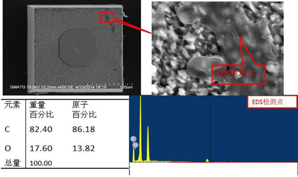
A client of red lamp bead found dark light problem, but have been unable to find out the reason, commissioned the analysis of failure reasons.After a series of instrumental analysis and elimination of packaging reasons, jin jian examined the bare crystal provided by the supplier and found that the luminous area of each chip contained pollutants of different areas. Energy spectrum analysis showed that the pollutant contained C and O, indicating that the pollutant was organic.We advise customers to pay attention to the production process specification and workshop environment of chip manufacturers, and strengthen the inspection of incoming materials.
Case study (ii) :
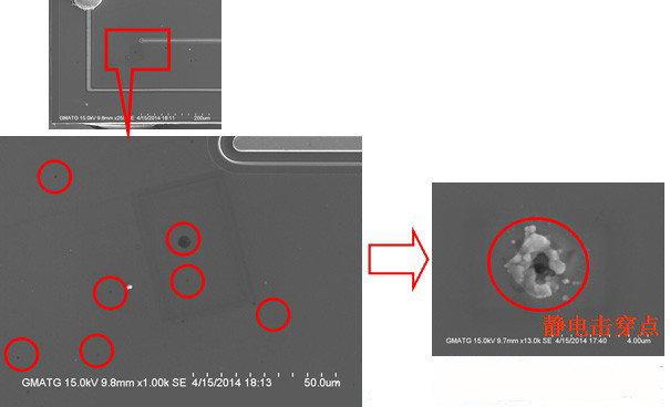
A customer produced a batch of lamp beads leakage problems, commissioned to find reasons.Through scanning electron microscopy, jin jian identified the electric leakage cause of these lamp beads as electrostatic breakdown and detected the bare crystal provided by the supplier. It was found that there were a large number of black holes on the surface of the chip epitaxial layer. These defects indicated that the epitaxial layer crystal quality was poor and there were defects inside the PN junction.Empty discovery, help the customer clear the responsible party of the accident, recover the loss for the customer.
Note: manufacturing process of LED chip
Manufacturing process flow chart of LED chip
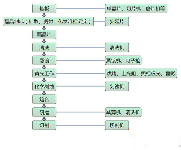
Epitaxial wafer - cleaning - plating transparent electrode layer and the transparent electrode lithography graphics - corrosion - to glue to platform graphics lithography, and dry etching to stripping, annealing SiO2 deposition - window graphics lithography - SiO2 corrosion - stripping - N extremely graphic lithography to pre cleaning, coating to peel, annealing to P extremely graphic printing, coating to peel, grinding and cutting to chip, finished product testing.
After growing into epitaxial wafers, the next step is to make electrodes (P pole, N pole) for the LED epitaxial wafers. Then, laser machine or diamond knife is used to cut the epitaxial wafers to make the chips. Then, nine points on different positions of the wafer are extracted for parameter testing.This is mainly to test voltage, wavelength, brightness, normal shipment of standard parameters of the wafer to continue the next operation, do not meet the requirements, on the side of another processing.After the wafer is cut into chips, 100% visual inspection (VI/VC) is required, and the operator is required to perform visual inspection under a 30 times magnification microscope.The chip is then selected, tested and classified by automatic classifier according to the predicted parameters of voltage, wavelength and brightness.Finally, LED chip inspection (VC) and labeling.The chip type, batch number, quantity and photoelectric measurement statistics are recorded on the label, attached to the back of the wax paper.The chip on the blue film will be the final visual test. The visual inspection standard is the same as the first time to ensure that the chip is arranged orderly and qualified.This is how LED chips are made.


.jpg)


 ChatNow